SRU Config
The Signal Routing Unit (SRU) is a hardware crossbar switch available on SHARC-FX processors that connects peripheral inputs and outputs to each other, and to and from external pins. The SRU Config tool lets you configure this routing graphically, removing the need to edit hardware registers directly.
The SRU Config tab only appears on the System Planner dashboard when the active System on Chip (SoC) is a SHARC-FX processor.
SRU Config overview
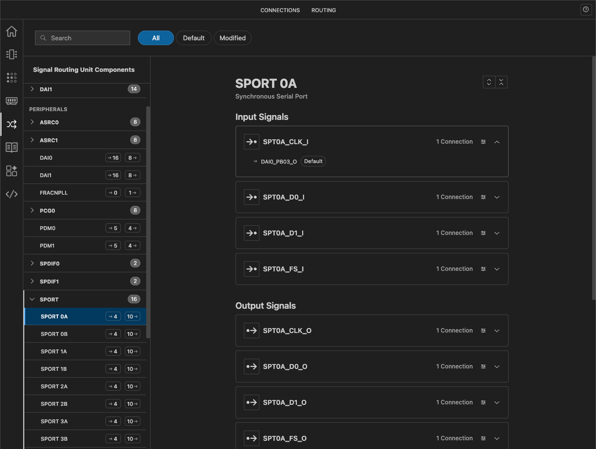
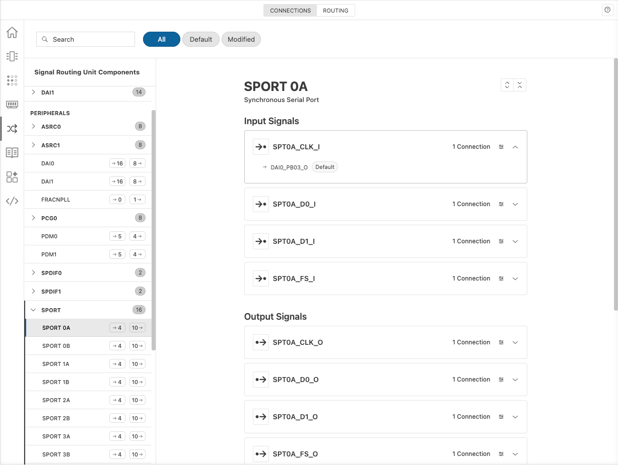
The SRU Config screen consists of two tabs:
- Connections – Configure routing one peripheral at a time, with a full connection details view for each signal.
- Routing – View and search all configured routes in a single table.
Connections tab
The Connections tab consists of several key components:
- Filter options: Use the search bar and filters to locate specific signals or peripherals, for example searching for
SPT0Aor filtering to only Modified signals. - Peripheral list: View available peripherals and pin buffers in the side panel. Select the chevron to expand a peripheral or pin buffer group and reveal its individual entries. Each entry shows its input and output signal counts as a pair of badges, for example
→ 4and10 →for four inputs and ten outputs. - Signal connections: Select an entry to view its input and output signals, for example the
SPT0A_CLK_Iinput andSPT0A_CLK_Ooutput of SPORT 0A (Synchronous Serial Port). - Connection Details panel: Select Configure

 on a signal to open the Connection Details panel and edit its routing.
Filter options
Use the Search field to find a signal or peripheral by name, alias, or description. When you enter a search term, a scope picker appears, letting you narrow the search to pin buffers, peripherals, signal names, or descriptions.
Use the All, Default, and Modified filter chips to show only signals with their default routing or only signals you've changed. When your search text has no results for a filter chip, that chip is unavailable and the current filter stays active.
Peripherals panel
The peripherals panel lists Pin Buffers and Peripherals as two separate groups.
Pin buffers are grouped by interface, for example DAI1 (Digital Applications Interface) on current SHARC-FX processors. Select the chevron to expand the group and reveal its individual entries. Each entry uses a shorter label than its full signal name, for example PB02 rather than DAI1_PB02_O.
Peripherals with multiple instances, such as SPORT, also appear as an expandable accordion group; select the group to expand it with the chevron and reveal its individual entries, for example SPORT 0A, SPORT 0B, and so on. Peripherals with a single instance appear as flat rows.
Each entry shows a name with a count of its input and output signals, shown as a pair of badges — for example → 4 and 10 → for four inputs and ten outputs.
Select the entry itself to view its signals in the main panel.
If the active SoC has no SRU peripherals or pin buffers available, the panel displays an empty state instead of the list.
Signal connections
Selecting a peripheral entry, such as SPORT 0A (Synchronous Serial Port), displays its signals as signal cards in the main panel, grouped into Input Signals and Output Signals. Within each of these, signals are further grouped by their signal type (for example Clock Signals or Data Signals) and sorted by name within each type group. Numeric portions are sorted by value, so SIGNAL2 appears before SIGNAL10. If no entry is selected, the main panel displays an empty state.
Select the chevron on a signal to expand it in place and view its current connection. Select the connected signal's name to jump to its card, if it has one — fixed sources such as LOW aren't selectable. A signal with no connections shows Unused instead of a connection count, and can't be expanded.
Each connection listed under an expanded output signal has an action. On a Modified connection, select Reset Source 
 to revert the input to its default routing, clear its description and alias, and reset its polarity to normal. On a Default connection, select Remove to disconnect the input by routing it to the fixed
LOW source while leaving its description, alias, and polarity unchanged.
Selecting a pin buffer entry, such as PB02, displays a Direction menu (Input, Output, or Bidirectional) and the fixed package Pin location for that pin buffer, for example DAI1_PIN02 (P18), above three sections in the main panel:
- Inputs shows the dedicated input signal of the pin buffer, for example
DAI1_PB02_I. - Outputs shows the dedicated output signal of the pin buffer, for example
DAI1_PB02_O. - Direction Controls shows the enable signal of the pin buffer, for example
DAI1_PBEN02_I.
Changing Direction changes what the enable signal is routed to, and updates the other signals of the pin buffer to match:
- Output routes the enable signal to a fixed HIGH source.
- Input routes the enable signal to a fixed LOW source.
- Bidirectional restores the last real signal that was routed to the enable signal, or opens a picker to select one if no real signal was routed to it before.
Editing a connection
Select Configure on a signal to open the Connection Details panel. The panel shows an input or output variant depending on the type of signal you select.
Input signal
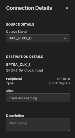
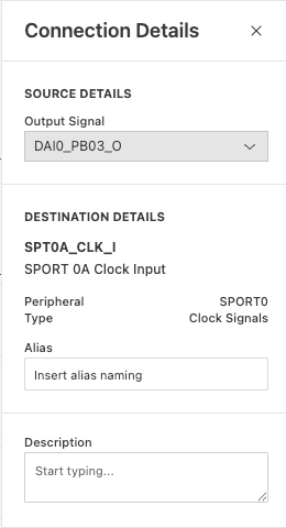
- Source Details has only an Output Signal picker to select the output that drives the input.
- Destination Details summarizes the input signal itself — its name, owning peripheral, and signal type — and includes its Alias field. Enter a name here to give the signal a custom display name. When a signal has an alias, CFS shows it as the primary label everywhere the signal appears — signal cards, the Connection Details panel, and picker fields — with the underlying signal name shown alongside it for reference. You can search for a signal by its alias or its name.
- Polarity control has an Invert signal polarity checkbox. Select it to invert the signal, or clear it to use the default normal polarity. Signal cards and the Routing tab mark an inverted connection as Modified, even when it uses its default source. The Connection Details panel for the output derives the input status only from its source, so the same connection can appear as Default there. This section only appears for an input signal whose SoC data model supports hardware polarity inversion, such as
DAI0_PB19_I. - Use Description to record a note about the input and its routing for anyone who reads the configuration later.
Output signal
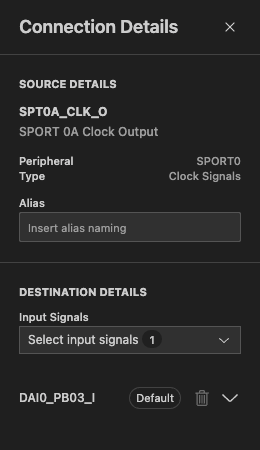
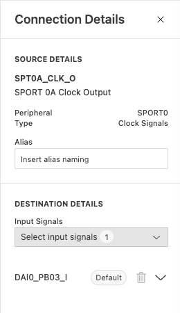
- Source Details summarizes the output signal itself and includes its Alias field (see Input signal for what an alias does).
- Destination Details has an Input Signals picker for adding inputs — an output can drive more than one input. Each connected input is also part of this section, as its own row:
- A Default or Modified badge shows whether the row is at its default routing (the routing the SoC ships with) or routing you've changed.
- Expand a row to edit that input's own Description. There's no single Description field for the output signal itself, since a single output can drive several inputs, each with its own description.
- Select Remove on a row to remove that connection. The input signal alias, if any, is unaffected. What removal does depends on the row:
- On a Modified row, it reverts the input to its default routing and clears the input signal description. The input signal polarity remains unchanged.
- On a Default row, it disconnects the input by routing it to the fixed
LOWsource and leaves the input signal description unchanged.
Note
Remove is unavailable when the default routing is already LOW, since there's nothing left to disconnect.
Edits are staged in the panel and only take effect when you select Save.
Warning
An output signal can drive more than one input. If you add an input that's already Modified — routed to a different output you (or someone else) previously changed — CFS shows a Reroute selected input? confirmation dialog before saving, listing the affected routing as <current output> → <input> and asking "Do you want to continue?" Select Confirm and Reroute to proceed.
Routing tab
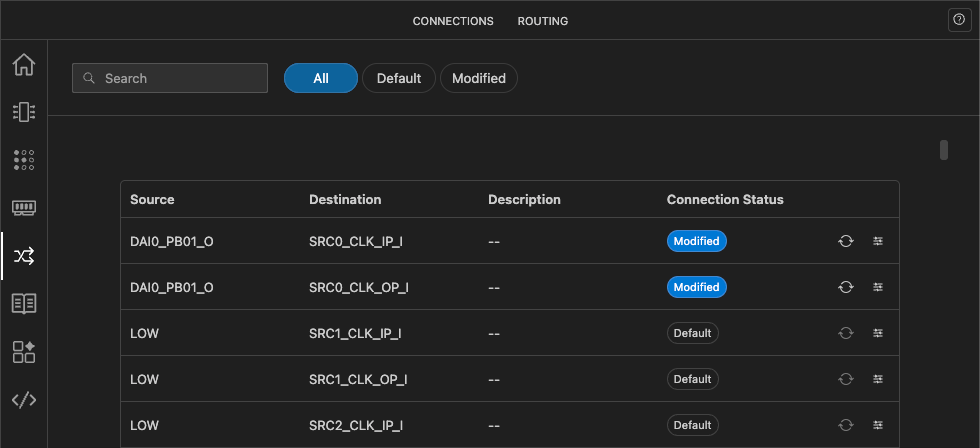
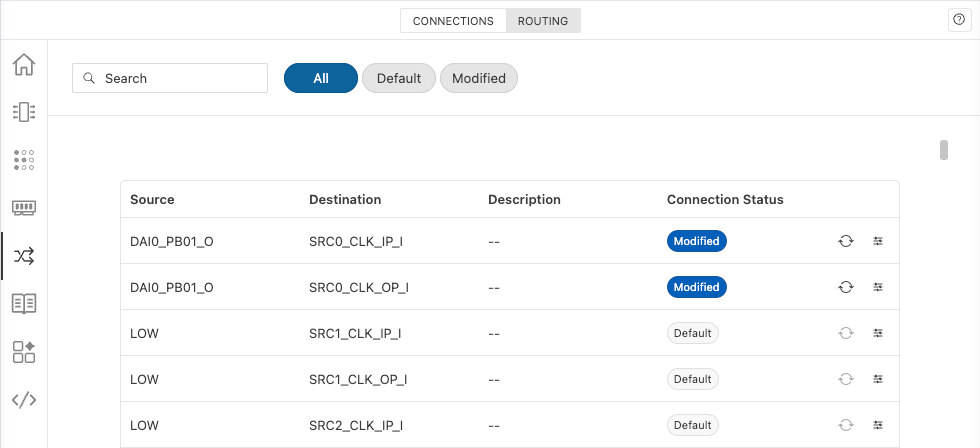
The Routing tab displays every configured connection in a single searchable table, rather than one peripheral at a time. Use the All, Default, and Modified filter chips to narrow the table, the same as on the Connections tab. The Search field here matches source and destination signal names and aliases only — it doesn't search descriptions, and there's no scope picker.
An Inverted Signal icon 
 appears next to the destination name for any input signal with polarity inversion enabled (see Input signal).
Use the Routing tab to review or audit all routing across the SoC. Use the Connections tab to configure or edit routing for a specific peripheral.
Each row has two actions:
- Reset Source

 – Reverts the routing of that input to its default, clears its Description and Alias, and resets its polarity to normal. Unavailable if the row already uses its default routing with normal polarity.
- Configure – Jumps directly to that signal's peripheral on the Connections tab, with the Connection Details panel already open.
Key concepts
- Signal: An input or output on an SRU-connected peripheral. Input signal names end in
_I; output signal names end in_O. - Pin buffer: A group of signals that connects a peripheral to and from an external pin — an input signal, an output signal, and an enable signal named with a
_PBEN##_Isuffix (for exampleDAI0_PBEN01_I) that controls whether the pin buffer drives the pin. - Connection: A route from an output signal (source) to an input signal (destination).
- Signal group: A peripheral instance, such as SPORT 0A, that groups the signals belonging to it. A signal group can contain multiple signal types, such as clock, data, or frame sync.
- Alias: An optional, user-defined custom name for a signal, shown alongside the underlying signal name.
- LOW / HIGH: Fixed logic-level sources, rather than routable signals. The default connections of a pin buffer tie its input signals to
LOWand its enable signal toHIGHorLOWdepending on pin direction, so unused pins default to a safe fixed state.
Next steps
After you select Save, CFS applies SRU connections, descriptions, and aliases to the open .cfsconfig editor. The file is marked as having unsaved changes until you save it, as with other System Planner edits. After configuring your SRU connections, use Generate Code to apply the desired configuration.