ADA4355
Overview
The purpose of this testbench is to validate the LVDS interface functionality of the projects/ada4355_fmc reference design.
The entire HDL documentation can be found here ADA4355-FMC HDL project.
Block design
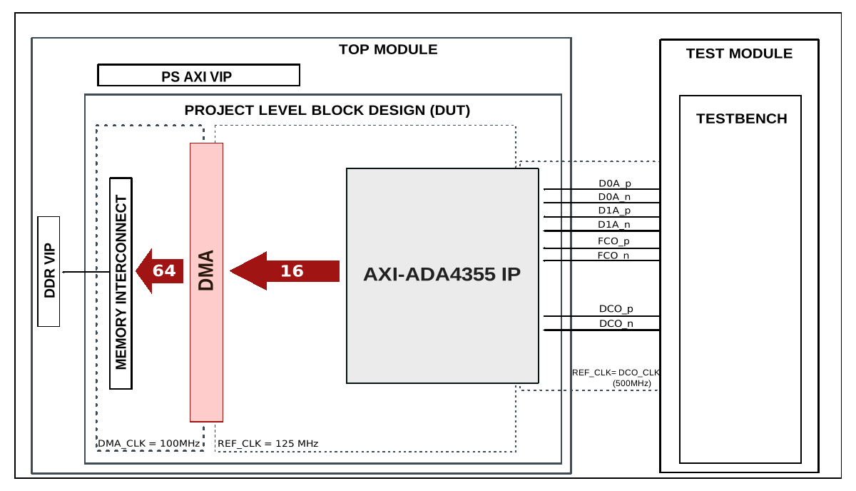
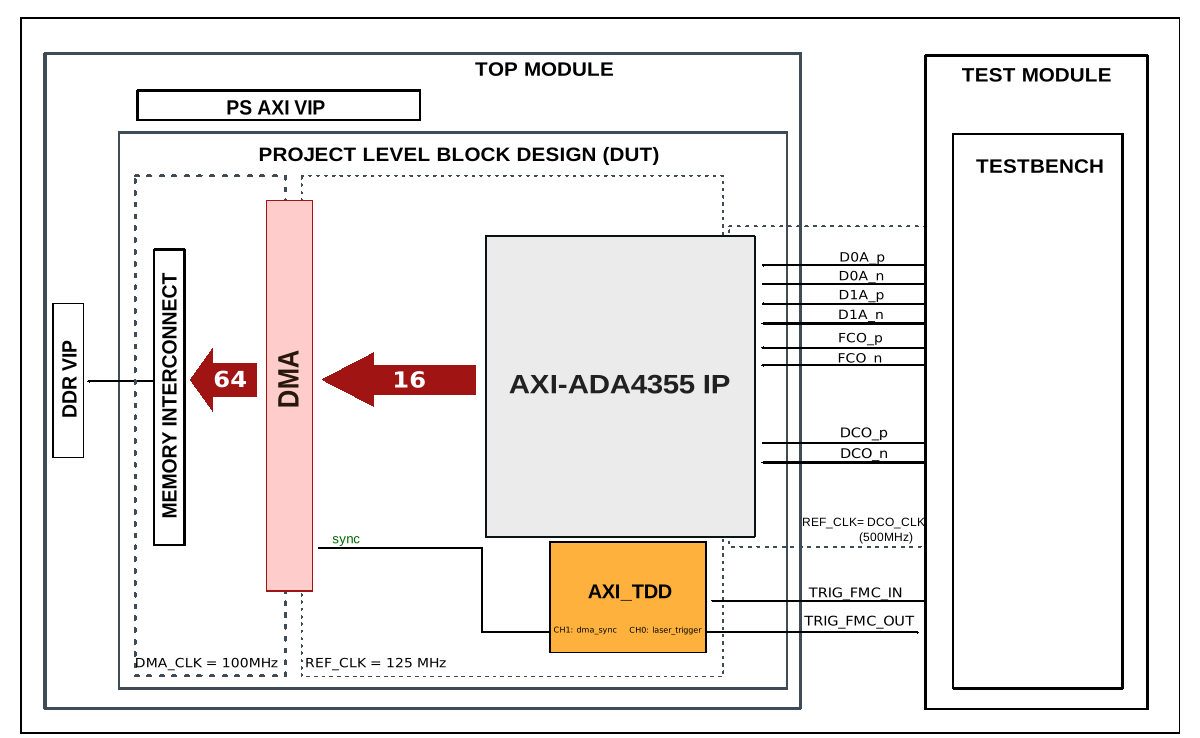
The testbench block design includes part of the ADA4355-FMC HDL reference design, along with VIPs used for clocking, reset, PS and DDR simulations.
Block diagram
The data path and clock domains are depicted in the below diagrams:
ADA4355 base configuration
ADA4356 TDD configuration
Configuration parameters and modes
The following parameters of this project that can be configured:
BUFMRCE_EN: used to differentiate between the ADA4355 and ADA4356 boards. Defines if the BUFMRCE primitive is used for clock gating: Options: 0 - Disabled (ADA4356), 1 - Enabled (ADA4355)
TDD_EN: enables the AXI TDD controller for LiDAR time-gated acquisition: Options: 0 - Disabled, 1 - Enabled
FRAME_SHIFT_CNT: defines the frame alignment shift count for testing different phase offsets between data and frame clock: Options: 0-7
Configuration files
The following configuration files are available:
Configuration mode |
Parameters |
||
|---|---|---|---|
BUFMRCE_EN |
TDD_EN |
FRAME_SHIFT_CNT |
|
cfg1 |
1 |
0 |
0 |
cfg2 |
0 |
0 |
0 |
cfg_tdd |
0 |
1 |
4 |
Tests
The following test program files are available:
Test program |
Usage |
|---|---|
test_program |
Tests the LVDS interface and DMA transfer capabilities. |
test_program_tdd |
Tests TDD-gated LiDAR acquisition with external sync trigger. |
Available configurations & tests combinations
Configuration |
Test |
Build command |
|---|---|---|
cfg1 |
test_program |
make CFG=cfg1 TST=test_program |
cfg2 |
test_program |
make CFG=cfg2 TST=test_program |
cfg_tdd |
test_program_tdd |
make CFG=cfg_tdd TST=test_program_tdd |
Error
Mixing a wrong pair of CFG and TST will result in a simulation error. Please check out the proposed combinations before running a custom test.
CPU/Memory interconnect addresses
Below are the CPU/Memory interconnect addresses used in this project:
Instance |
Address |
|---|---|
axi_intc |
0x4120_0000 |
axi_ada4355_adc |
0x44A0_0000 |
axi_ada4355_dma |
0x44A3_0000 |
axi_tdd_0 * |
0x44A4_0000 |
ddr_axi_vip |
0x8000_0000 |
Legend
*instantiated only when TDD_EN=1
Interrupts
Below are the Programmable Logic interrupts used in this project:
Instance name |
HDL |
|---|---|
axi_ada4355_dma |
13 |
Test stimulus
test_program
The test program is structured into several tests as follows:
Environment bringup
The steps of the environment bringup are:
Create the environment
Start the environment
Start the clocks
Assert the resets
Sanity test
This test is used to check the communication with the DMA module by running the DMA API sanity test.
DMA test
The DMA test verifies the data capture path from the LVDS interface through the AXI DMAC.
The steps of this test are:
Configure the ADC interface (set control registers, number of lanes, DDR mode)
Release the ADC from reset and assert sync_n to start data capture
Configure the DMA (enable, set flags, transfer length, destination address)
Start the DMA transfer
Enable the frame pattern for data alignment
Wait for DMA transfer completion
Verify that captured data matches the expected sine wave pattern
Resync test
The resync test verifies that the FSM can re-align after a sync pulse.
The steps of this test are:
Pulse sync_n low to trigger FSM reset
Wait for FSM to complete alignment search
Verify that the FSM has re-aligned correctly
test_program_tdd
The TDD test program extends the base test with LiDAR time-gated acquisition. It is structured into several tests as follows:
Environment bringup
Same as the base test program.
Sanity test
Same as the base test program.
DMA test with TDD
The DMA test configures the AXI TDD controller for time-gated acquisition.
The steps of this test are:
Configure the ADC interface and start data capture
Configure the AXI TDD controller (frame length, channels, sync settings)
Configure the DMA with sync transfer start enabled
Trigger the TDD via external sync pulse
Wait for DMA transfer completion
Verify that captured data matches the expected sine wave pattern
TDD LiDAR test
The TDD LiDAR test verifies the full time-gated acquisition cycle with realistic LiDAR timing parameters.
The steps of this test are:
Configure the ADC interface and start data capture
Reset the TDD controller FSM
Configure TDD timing: CH0 for laser trigger pulse, CH1 for DMA sync
Configure and arm the DMA with sync transfer start
Enable frame pattern for data alignment
Trigger the TDD via external sync pulse
Wait for DMA transfer completion
Verify that captured data matches the expected sine wave pattern
Building the testbench
The testbench is built upon ADI’s generic HDL reference design framework. ADI does not distribute compiled files of these projects so they must be built from the sources available here and here, with the specified hierarchy described Set up the Testbenches repository. To get the source you must clone the HDL repository, and then build the project as follows:.
Linux/Cygwin/WSL
Example 1
Build all the possible combinations of tests and configurations, using only the command line.
user@analog:~$
cd testbenches/project/ada4355
user@analog:~/testbenches/project/ada4355$
make
Example 2
Build all the possible combinations of tests and configurations, using the Vivado GUI. This command will launch Vivado, will run the simulation and display the waveforms.
user@analog:~$
cd testbenches/project/ada4355
user@analog:~/testbenches/project/ada4355$
make MODE=gui
Example 3
Build a particular combination of test and configuration, using the Vivado GUI. This command will launch Vivado, will run the simulation and display the waveforms.
user@analog:~$
cd testbenches/project/ada4355
user@analog:~/testbenches/project/ada4355$
make MODE=gui CFG=cfg1 TST=test_program
The built projects can be found in the runs folder, where each configuration
specific build has it’s own folder named after the configuration file’s name.
Example: if the following command was run for a single configuration in the
clean folder (no runs folder available):
make CFG=cfg1
Then the subfolder under runs name will be:
cfg1
Resources
More information
Support
Analog Devices, Inc. will provide limited online support for anyone using the reference design with ADI components via the EngineerZone FPGA reference designs forum.
It should be noted, that the older the tools’ versions and release branches are, the lower the chances to receive support from ADI engineers.