AD738x
Overview
The purpose of this testbench is to validate the serial interface functionality of the projects/ad738x_fmc reference design.
The entire HDL documentation can be found here AD738x-FMC HDL project.
Block design
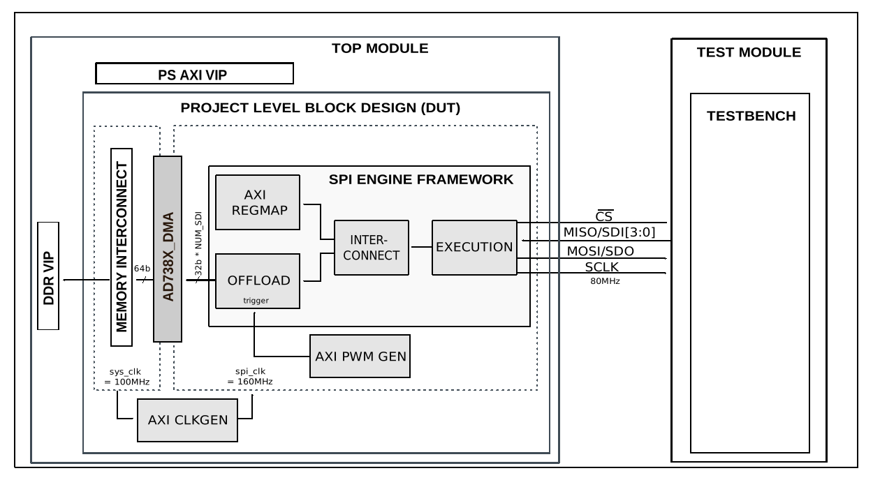
The testbench block design includes part of the AD738x-FMC HDL reference design, along with VIPs used for clocking, reset, PS and DDR simulations.
Block diagram
The data path and clock domains are depicted in the below diagram:
Configuration parameters and modes
The following parameters of this project that can be configured:
ALERT_SPI_N: defines if a known pin will operate as a serial data output pin or alert indication pin: Options: 0 - Serial Data Output Pin, 1 - Alert Indication Ouput Pin
NUM_OF_SDIO: defines the number of MOSI lines of the SPI interface: Options: 1 - Interleaved mode, 2 - 1 lane per channel, 4 - 2 lanes per channel
Configuration files
The following configuration files are available:
Configuration mode
Parameters
ALERT_SPI_N | NUM_OF_SDIO
cfg1
0
2
Tests
The following test program file is available:
Test program |
Usage |
|---|---|
test_program |
Tests the serial interface capabilities. |
Available configurations & tests combinations
The test program is compatible with the above mentioned configuration.
CPU/Memory interconnect addresses
Below are the CPU/Memory interconnect addresses used in this project:
Instance |
Address |
|---|---|
spi_ad738x_adc_axi_regmap |
0x44A0_0000 |
axi_ad738x_dma |
0x44A3_0000 |
spi_clkgen |
0x44A7_0000 |
spi_trigger_gen |
0x44B0_0000 |
Interrupts
Below are the Programmable Logic interrupts used in this project:
Instance name |
HDL |
|---|---|
axi_ad738x_dma |
13 |
spi_ad738x_adc |
12 |
Test stimulus
The test program is structured into several tests as follows:
Environment bringup
The steps of the environment bringup are:
Create the environment
Start the environment
Start the clocks
Assert the resets
Sanity test
This test is used to check the communication with the AXI REGMAP module of the AD738X SPI Engine interface, by reading the core VERSION register, along with writing and reading the SCRATCH register.
FIFO SPI test
The FIFO SPI test verifies the simple serial transfers, made through the Execution module.
The steps of this test are:
Start the SPI clock generator (axi_clkgen)
Enable SPI Engine & configure the Execution module
Set up the interrupts
Generate a FIFO transaction
Capture and compare the results, using the PEEK register of the AXI SPI Engine
Offload SPI test
The Offload SPI test verifies the Offload module functionality.
The steps of this test are:
Configure the conversion signal generator (axi_pwmgen)
Configure the DMA
Configure the Offload module
Start the Offload module
Capture and compare the Offload SDI data
Stop the environment
Stop the clocks
Building the testbench
The testbench is built upon ADI’s generic HDL reference design framework. ADI does not distribute compiled files of these projects so they must be built from the sources available here and here, with the specified hierarchy described Set up the Testbenches repository. To get the source you must clone the HDL repository, and then build the project as follows:.
Linux/Cygwin/WSL
Example 1
Build all the possible combinations of tests and configurations, using only the command line.
user@analog:~$
cd testbenches/project/ad738x
user@analog:~/testbenches/project/ad738x$
make
Example 2
Build all the possible combinations of tests and configurations, using the Vivado GUI. This command will launch Vivado, will run the simulation and display the waveforms.
user@analog:~$
cd testbenches/project/ad738x
user@analog:~/testbenches/project/ad738x$
make MODE=gui
Example 3
Build a particular combination of test and configuration, using the Vivado GUI. This command will launch Vivado, will run the simulation and display the waveforms.
user@analog:~$
cd testbenches/project/ad738x
user@analog:~/testbenches/project/ad738x$
make MODE=gui CFG=cfg1 TST=test_program
The built projects can be found in the runs folder, where each configuration
specific build has it’s own folder named after the configuration file’s name.
Example: if the following command was run for a single configuration in the
clean folder (no runs folder available):
make CFG=cfg1
Then the subfolder under runs name will be:
cfg1
Resources
More information
Support
Analog Devices, Inc. will provide limited online support for anyone using the reference design with ADI components via the EngineerZone FPGA reference designs forum.
It should be noted, that the older the tools’ versions and release branches are, the lower the chances to receive support from ADI engineers.